Close
- Information Technology
- Data Infrastructure
- Data Tools
- Desktops, Laptops and OS
- Chip Sets
- Collaboration Tools
- Desktop Systems - PCs
- Email Client
- Embedded Systems
- Hardware and Periferals
- Laptops
- Linux - Open Source
- Mac OS
- Memory Components
- Mobile Devices
- Presentation Software
- Processors
- Spreadsheets
- Thin Clients
- Upgrades and Migration
- Windows 7
- Windows Vista
- Windows XP
- Word Processing
- Workstations
- Enterprise Applications
- IT Infrastructure
- IT Management
- Networking and Communications
- Bluetooth
- DSL
- GPS
- GSM
- Industry Standard Protocols
- LAN - WAN
- Management
- Mobile - Wireless Communications
- Network
- Network Administration
- Network Design
- Network Disaster Recovery
- Network Interface Cards
- Network Operating Systems
- PBX
- RFID
- Scalability
- TCP - IP
- Telecom Hardware
- Telecom Regulation
- Telecom Services
- Telephony Architecture
- Unified Communications
- VPNs
- VoIP - IP Telephony
- Voice Mail
- WAP
- Wi-Fi (802.11)
- WiMAX (802.16)
- Wide Area Networks (WAN)
- Wireless Internet
- Wireless LAN
- Security
- Servers and Server OS
- Software and Web Development
- .Net Framework
- ASPs
- Application Development
- Application Servers
- Collaboration
- Component-Based
- Content Management
- E-Commerce - E-Business
- Enterprise Applications
- HTML
- IM
- IP Technologies
- Integration
- Internet
- Intranet
- J2EE
- Java
- Middleware
- Open Source
- Programming Languages
- Quality Assurance
- SAAS
- Service-Oriented Architecture (SOA)
- Software Engineering
- Software and Development
- Web Design
- Web Design and Development
- Web Development and Technology
- XML
- Storage
- Agriculture
- Automotive
- Career
- Construction
- Education
- Engineering
- Broadcast Engineering
- Chemical
- Civil and Environmental
- Control Engineering
- Design Engineering
- Electrical Engineering
- GIS
- General Engineering
- Industrial Engineering
- Manufacturing Engineering
- Materials Science
- Mechanical Engineering
- Medical Devices
- Photonics
- Power Engineering
- Process Engineering
- Test and Measurement
- Finance
- Food and Beverage
- Government
- Healthcare and Medical
- Human Resources
- Information Technology
- Data Infrastructure
- Data Tools
- Desktops, Laptops and OS
- Chip Sets
- Collaboration Tools
- Desktop Systems - PCs
- Email Client
- Embedded Systems
- Hardware and Periferals
- Laptops
- Linux - Open Source
- Mac OS
- Memory Components
- Mobile Devices
- Presentation Software
- Processors
- Spreadsheets
- Thin Clients
- Upgrades and Migration
- Windows 7
- Windows Vista
- Windows XP
- Word Processing
- Workstations
- Enterprise Applications
- IT Infrastructure
- IT Management
- Networking and Communications
- Bluetooth
- DSL
- GPS
- GSM
- Industry Standard Protocols
- LAN - WAN
- Management
- Mobile - Wireless Communications
- Network
- Network Administration
- Network Design
- Network Disaster Recovery
- Network Interface Cards
- Network Operating Systems
- PBX
- RFID
- Scalability
- TCP - IP
- Telecom Hardware
- Telecom Regulation
- Telecom Services
- Telephony Architecture
- Unified Communications
- VPNs
- VoIP - IP Telephony
- Voice Mail
- WAP
- Wi-Fi (802.11)
- WiMAX (802.16)
- Wide Area Networks (WAN)
- Wireless Internet
- Wireless LAN
- Security
- Servers and Server OS
- Software and Web Development
- .Net Framework
- ASPs
- Application Development
- Application Servers
- Collaboration
- Component-Based
- Content Management
- E-Commerce - E-Business
- Enterprise Applications
- HTML
- IM
- IP Technologies
- Integration
- Internet
- Intranet
- J2EE
- Java
- Middleware
- Open Source
- Programming Languages
- Quality Assurance
- SAAS
- Service-Oriented Architecture (SOA)
- Software Engineering
- Software and Development
- Web Design
- Web Design and Development
- Web Development and Technology
- XML
- Storage
- Life Sciences
- Lifestyle
- Management
- Manufacturing
- Marketing
- Meetings and Travel
- Multimedia
- Operations
- Retail
- Sales
- Trade/Professional Services
- Utility and Energy
- View All Topics
Share Your Content with Us
on TradePub.com for readers like you. LEARN MORE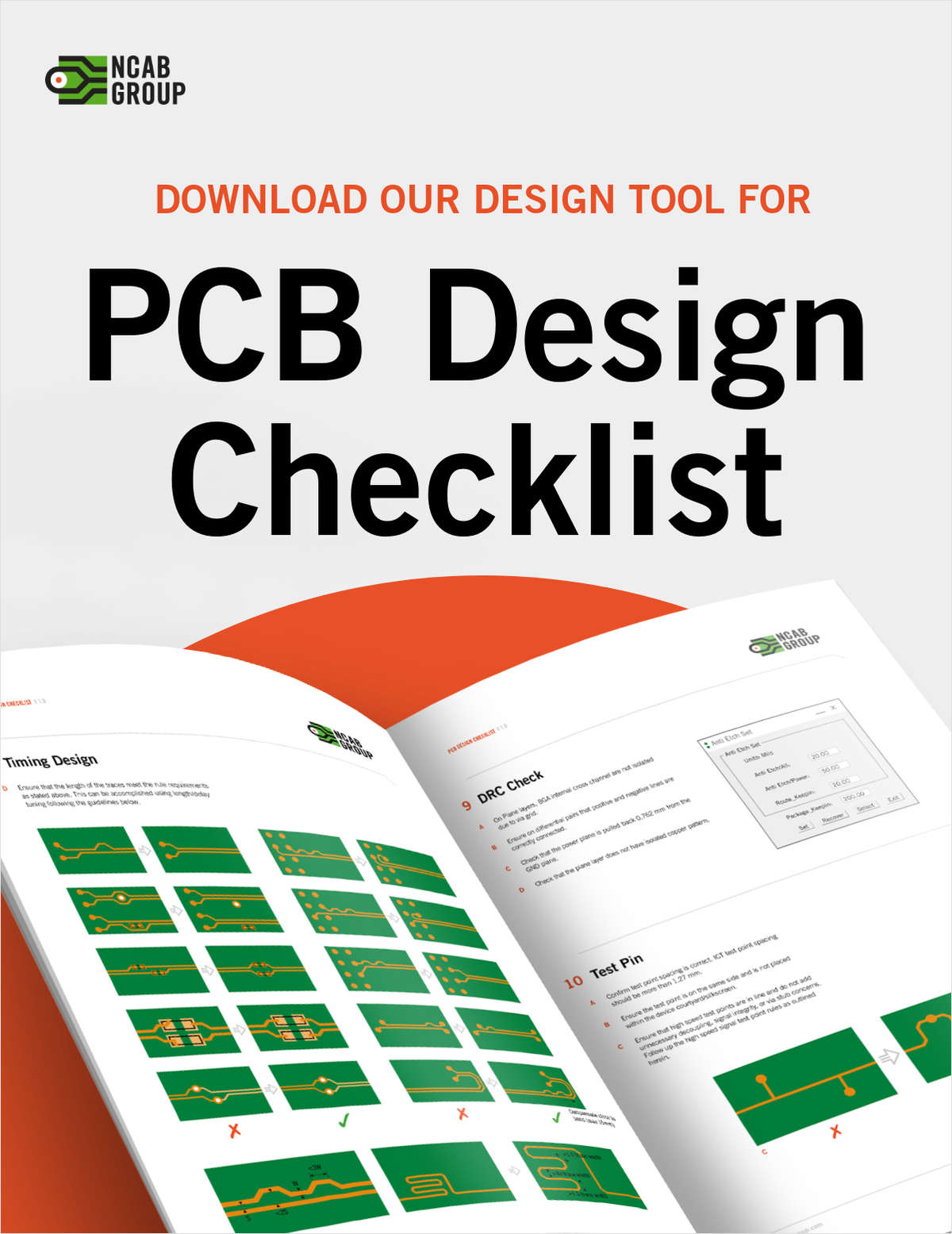

Request Your Free Guide Now:
"PCB Design Checklist"
When your PCB has been designed you probably want to start the production right away. But take some time to first take a look and make sure the critical areas of the design are covered.
Is your solder mask larger than the component pad? Have you considered any possible mechanical assembly problems using a 3D model of the assembly? To help you with this, we created the PCB design checklist. This checklist can aid you in your own design work. Alongside our PCB design guidelines, this will provide a total solution to further help you get it right from the start.
Offered Free by: NCAB Group
See All Resources from: NCAB Group
Recommended for Professionals Like You:

Thank you
This download should complete shortly. If the resource doesn't automatically download, please, click here.


Thank you
This download should complete shortly. If the resource doesn't automatically download, please, click here.